In the world of scanning probe microscopy, newer doesn’t always mean better. The Agilent 5100 (PicoLE) SPM System—originally developed under the Molecular Imaging brand and later carried forward by Agilent and Keysight—remains one of the most trusted entry-level platforms in academic and industrial labs. Its combination of accessible price point, versatile imaging modes, and cross-generational compatibility has made it a quiet workhorse in surface science for over two decades.
In this post, we take a closer look at what makes the 5100 (PicoLE) system tick, where it has been used in published research, and how labs can continue getting the most out of this reliable platform.
What Is the 5100 (PicoLE)?
The 5100 PicoLE is a compact, entry-level Scanning Probe Microscope (SPM) designed for core imaging applications. It supports the fundamental AFM and SPM modes that most surface characterization tasks require, making it ideal for research groups that need reliable, repeatable nanoscale imaging without the overhead of a flagship system.
One of its defining strengths is cross-manufacturer continuity. As the platform transitioned from Molecular Imaging → Agilent → Keysight, component compatibility was preserved across generations. This means labs that purchased the system years ago can still source compatible scanners, controllers, and accessories—including through specialist suppliers like AFM-Parts.com.
System Highlights
Entry-level SPM with proven reliability
Supports core AFM/STM/SPM imaging modes
Compatible with Molecular Imaging, Agilent & Keysight
Accessible cost point for academic labs
Long-term parts & support availability
Suitable for both research & teaching environments
The 5100 PicoLE in Published Research
The best validation for any scientific instrument is where it shows up in the literature. A compelling example comes from a 2013 multi-laboratory study published in Langmuir (ACS Publications), in which researchers from institutions including KU Leuven, EPFL, Université de Strasbourg, and the University of Geneva used multiple STM platforms to image the same nanoparticle samples. The Agilent 5100 (PicoLE) was one of the instruments used at KU Leuven, alongside a Bruker Multimode.
The study’s central finding was striking: STM images of mixed-ligand gold nanoparticles acquired across different laboratories, different operators, and different microscopes—including the 5100—showed reproducible structural features at the nanoscale. When analyzed using power spectral density (PSD) methods, characteristic length scales of approximately 1.2 nm were consistent across all instruments, regardless of imaging parameters or scan speed.
“Images of mixed-ligand NPs recorded in different laboratories under different conditions with different operators, instruments, and time all exhibit [the same structural features].”
— Biscarini et al., Langmuir, 2013 (ACS Publications, open access)
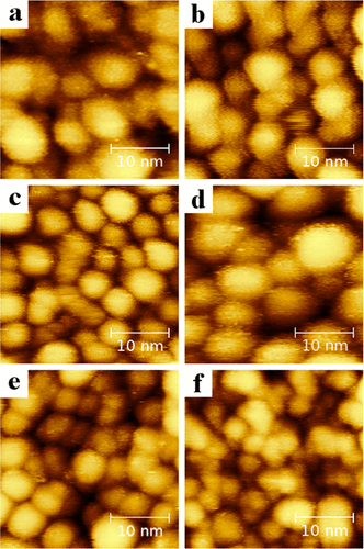
For labs evaluating whether the 5100 PicoLE can produce publication-quality data: this study shows it standing shoulder-to-shoulder with instruments from Bruker and Omicron in a rigorous, multi-site comparison. The ability to cross-validate findings across platforms is a testament to the 5100’s measurement fidelity.
Who Is the 5100 (PicoLE) For?
Over the years, the 5100 has found a home in a variety of environments:
University Research Labs
Ideal for groups that need a dependable SPM system for surface morphology studies, thin film characterization, or materials science research.
Teaching & Training
The 5100’s approachable design and robust construction make it well-suited for student training programs in nanotechnology and surface science.
Core Facility Upgrades
Labs looking to maintain or upgrade existing 5100 systems rather than replace them entirely—maximizing their original investment.
Keeping Your 5100 Running: Parts & Compatibility
One of the more practical challenges facing owners of legacy SPM systems is parts availability. As original manufacturers shift focus to newer platforms, sourcing replacement scanners, controllers, or optical accessories for older systems can become difficult.
At AFM-Parts.com, we specialize in exactly this gap. Our inventory for the 5100 (PicoLE) platform includes:
- Complete 5100 (PicoLE) base systems
- Compatible scanners including STM scanner units
- Navitar optical access upgrades for the 5100/5500 series
- Controllers and electronics modules
- Probe holders and tips
All components are tested for cross-compatibility across Molecular Imaging, Agilent, and Keysight generations, so you can mix and match with confidence.
Looking for 5100 (PicoLE) Parts or a Complete System?
We currently have 2 units in stock. Request a quote or ask a technical question—our team responds quickly.
Tips for Getting the Best Results from Your 5100
Whether you’re a first-time user or returning to the platform after years away, a few practical reminders can make a significant difference in image quality:
The multi-lab Langmuir study mentioned above noted that leaving the microscope scanning continuously for at least 12 hours before acquiring critical data significantly improved thermal stability and minimized piezo scanner hysteresis.
Excessive integral or proportional gain introduces feedback loop oscillations that can mimic genuine surface features in STM mode. If you see suspicious periodic patterns, lower the gains before drawing conclusions.
Power spectral density analysis (available in open-source tools like Gwyddion) is a powerful operator-independent method for extracting reproducible morphological information from SPM images—particularly useful when comparing data across sessions or instruments.
When imaging small features, reducing the scanner’s z dynamic range to the minimum needed for your sample enhances vertical resolution—an often-overlooked setting that can dramatically improve the detail visible on nanostructures.
Conclusion
The Agilent 5100 (PicoLE) SPM System is a testament to the principle that well-engineered scientific instruments age gracefully. Its presence in multi-institutional published research, its cross-manufacturer compatibility, and its continued use in teaching and research labs worldwide speak to a platform that was built with real science in mind.
For labs that own one and want to keep it operational, quality replacement parts and upgrades are available. For labs looking to acquire a capable entry-level SPM at a fraction of new system costs, refurbished 5100 units offer compelling value.
Have questions about compatibility, available stock, or technical specifications? Get in touch with our team—we’re happy to help.
Topics:
AFM Systems · Agilent · Keysight · Molecular Imaging · Scanning Probe Microscopy · STM · Nanocharacterization · Legacy Systems